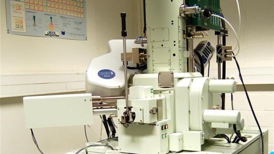
(Field Emmission) Secondary Electron Spectroscopy
Principle and characterization possibilities
In the scanning electron microscope a stream of primary electrons is focused onto the sample surface resulting in a number of different particles or waves being emitted (secondary electrons, back- scattered electrons, X-rays, photons, Auger electrons...). The secondary and backscattered electrons are used for imaging while the X-rays give characteristic chemical information of the emitting atoms (EDS/WDX). The probed depth in EDX/WDX analysis is around 1-3 μm.
Available instruments and specifications
JEOL JSM-7100F
- Field Emission source
- lateral resolution of 1.2 nm at 30 kV, 3 nm at 1 kV and 3.0 nm at 15 kV
- WDX spectrometer (energy resolution 10eV)
- integrated SDD X-MaxN 20 mm2 EDS detector (energy resolution 127eV)
Jeol JSM-IT300
- Tungsten filament source
- low vacuum module, pressures up to 650Pa
- lateral resolution of 3 nm at 30 kV, 15 nm at 1 kV (high vacuum)
- lateral resolution of 4 nm at 30 kV (low vacuum)
- EDS detector (energy resolution 127eV)

Atomic Force Microscopy
Principle and characterization possibilities
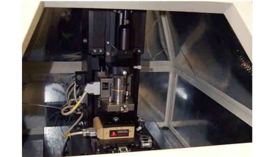
Atomic force microscopy is a method of sample surface topography imaging. The topography image is observed by means of forces between a sharp AFM tip and the sample surface atoms in the order of nano Newtons.
Through microfabrication technology nano sized needles (tips) are placed at the end of Si springs and are used as force sensors. AFM systems also have laser subsystems. The laser beam is focused at the tip edge and the deflection of the beam can be measured with a photodetector. When the tip scans the sample surface, the force between surface atoms and tip is kept constant by using a feedback system. The measured tip movement gives the surface topography image of the sample.
AFM systems have different application areas that depend on material properties, e.g., abrasion, monolayer formation, magnetic properties, surface roughness... Electrochemical scans can also be carried out on a nano scale to study corrosion mechanisms, mono layer formation, initiation hotspots...
Available instruments and specifications
Park XE-100
- Automated system
- Scanning Kelvin Probe option
- Electrochemical in situ system available
- Maximum 100μm x 100μm scan area
Park XE-10
- Maximum 100μm x 100μm scan area
- In glovebox environment
Park NX-10
- Maximum 100μm x 100μm scan area
- In dry-room environment
- Scanning Kelvin Probe option
AAN TE VULLEN FYSC AFMs

